- 您现在的位置:买卖IC网 > Sheet目录484 > NOIL1SE3000A-GDC (ON Semiconductor)IC IMAGE SENSOR 3MP 369-PGA
�� �
�
�NOIL1SN3000A�
�Y_end� (b0001001� /� d9� and� b0001010� /� d10)�
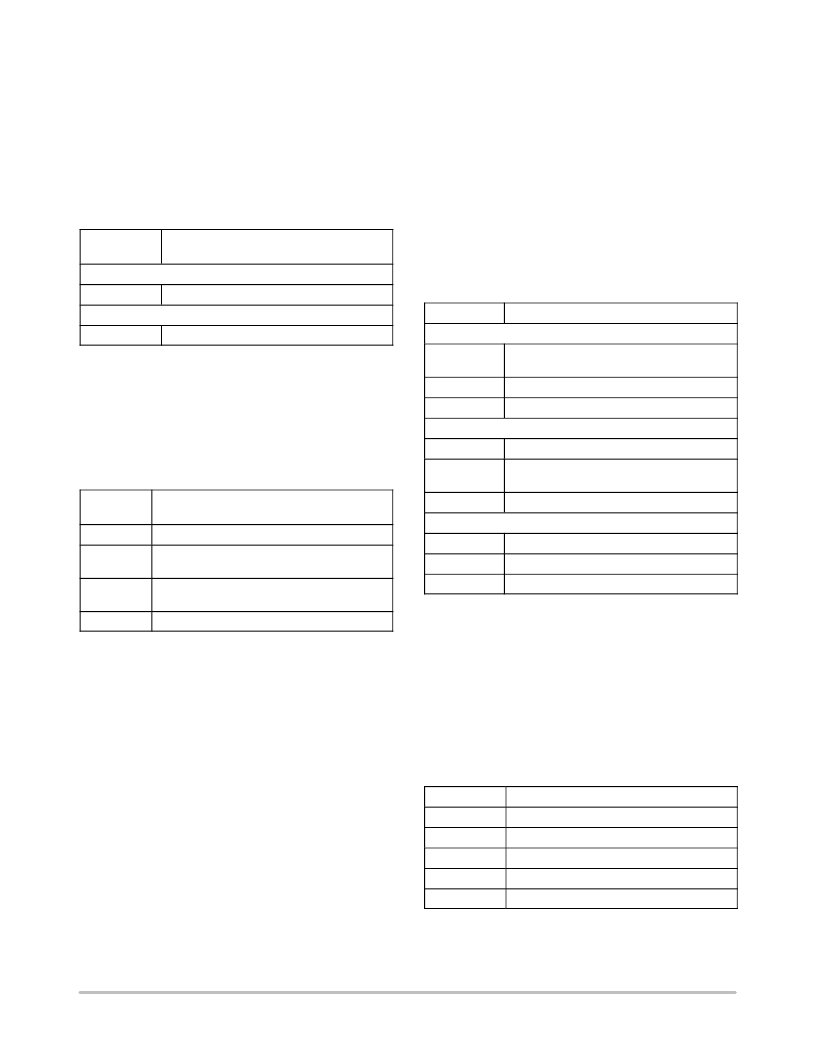
�The� Y_end� register� contains� the� row� address� of� the� last�
�row� to� readout.� Because� a� row� address� is� 11-bit� wide,� the�
�Y_end� address� is� split� over� two� registers:� Y_end<10:8>� and�
�Y_end<7:0>.� Y_end<10:8>� contains� 3� MSBs� of� the� 11-bit�
�address,� and� Y_end<7:0>� contains� 8� LSBs� of� the� address.�
�Y_end<10:0>� must� be� larger� than� Y_start<10:0>� and� not�
�larger� than� 1709.�
�Training� (b0001100� /� d12)�
�This� register� allows� switching� between� different� readout�
�modes.� Bits� <7:2>� are� ignored.�
�?� Training_en,� bit<0>� .� In� bypass� mode,� this� bit� is�
�evaluated� and� determines� if� the� training� pattern� or� test�
�image� is� transmitted.�
�?� Bypass_mode,� bit<1>� .� This� bit� allows� the� sensor� to�
�switch� between� normal� readout� of� an� image� and� readout�
�Table� 24.� Y_END� REGISTER�
�Value�
�Bit<2:0>�
�Y_end<7:0>� (b0001001� /� d9)�
�Effect�
�for� testing� or� training� purposes.�
�?� Analog_out_en,� bit<2>� .This� bit� activates� the� analog�
�output� of� the� sensor.� The� analog� value� of�
�column<1696>� is� brought� to� the� output.�
�On� startup�
�10101101�
�Table� 26.� TRAINING� REGISTER�
�Y_end<10:8>� (b0001010� /� d10)� :� Bits<7:3>� are� ignored�
�Value�
�Effect�
�On� startup�
�00000110�
�Training_en,� bit<0>�
�X_start� (b0001011� /� d11)�
�The� X_start� register� contains� the� start� position� for� the� X�
�1�
�0�
�In� bypass� mode,� the� training� pattern� is�
�transmitted�
�In� bypass� mode,� the� test� image� is� transmitted�
�readout.� Readout� in� X� starts� only� at� odd� kernel� positions.� As�
�a� result,� possible� start� positions� are� 64� columns� (2� kernels)�
�separated� from� each� other.�
�On� startup� 0�
�Bypass_mode,� bit<1>�
�Bits� <7:5>� are� ignored.�
�Table� 25.� X_START� REGISTER�
�0�
�1�
�Normal� readout� of� captured� images�
�Bypass� mode� readout.� The� content� of� register�
�TRAINING_EN� is� evaluated.�
�Value�
�Bit<4:0>�
�00000�
�00001�
�Effect�
�X� readout� starts� with� the� first� kernel� (column� 0)�
�X� readout� starts� with� the� third� kernel�
�(column� 64)�
�On� startup� 0�
�Analog_out_en,� bit<2>�
�0� Analog� output� disabled�
�1� Analog� output� enabled�
�11010�
�X� readout� starts� with� the� fifty� third� kernel�
�(column� 1664)�
�On� startup�
�0�
�On� startup�
�00000�
�Black_ref� (b0001101� /� d13)�
�This� register� controls� the� DAC� that� sets� the� dark� level� for�
�the� ADC.� The� analog� output� of� the� DAC� corresponds� with�
�the� all� zero� code� of� the� ADC.� The� DAC� has� an� 8-bit�
�resolution� and� outputs� between� VAA2V5� and� 0� V.� This�
�means� that� the� step� size� corresponds� with� about� 9.8� mV.� The�
�DAC� itself� outputs� between� VAA2V5� and� 0� V,� but� the�
�buffering� circuit� that� follows� after� the� DAC� clips� the� voltage�
�close� to� ground� and� supply.�
�Table� 27.� BLACK_REF� REGISTER�
�Value�
�Effect�
�00000000�
�Output� of� DAC� is� VAA2V5�
�00000001�
�Output� of� DAC� is� VAA2V5–9.8� mV�
�…�
�11111111�
�Output� of� DAC� is� 0� V�
�On� startup�
�01100110�
�http://onsemi.com�
�23�
�发布紧急采购,3分钟左右您将得到回复。
相关PDF资料
NOIL1SM0300A-WWC
IC IMAGE SENSOR LUPA300 48LLC
NOIL2SC1300A-GDC
IC IMAGE SENSOR LUPA1300 168PGA
NOIV1SE025KA-GDC
IC IMAGE SENSOR 25MP 355PGA
NP100P04PDG-E1-AY
MOSFET P-CH -40V MP-25ZP/TO-263
NP100P04PLG-E1-AY
MOSFET P-CH -40V MP-25ZP/TO-263
NP100P06PDG-E1-AY
MOSFET P-CH -60V MP-25ZP/TO-263
NP100P06PLG-E1-AY
MOSFET P-CH -60V MP-25ZP/TO-263
NP109N04PUJ-E1B-AY
MOSFET N-CH 40V MP-25ZP/TO-263
相关代理商/技术参数
NOIL1SM0300A-QDC
功能描述:IC IMAGE SENSOR LUPA300 48LLC RoHS:是 类别:传感器,转换器 >> 图像,相机 系列:* 标准包装:480 系列:- 象素大小:6.7µm x 6.7µm 有源象素阵列:768H x 488V 每秒帧数:52 电源电压:3.3V 类型:CMOS 成像 封装/外壳:48-QFP 供应商设备封装:48-QFP 包装:托盘 请注意:* 配用:4H2105-ND - HEADBOARD FOR KAC-004014H2104-ND - KIT EVAL FOR KAC-00401 其它名称:4H20954H2095-NDKAC-00401-CBC-LB-A0
NOIL1SM0300A-WWC
功能描述:IC IMAGE SENSOR LUPA300 48LLC RoHS:是 类别:传感器,转换器 >> 图像,相机 系列:LUPA300 标准包装:480 系列:- 象素大小:6.7µm x 6.7µm 有源象素阵列:768H x 488V 每秒帧数:52 电源电压:3.3V 类型:CMOS 成像 封装/外壳:48-QFP 供应商设备封装:48-QFP 包装:托盘 请注意:* 配用:4H2105-ND - HEADBOARD FOR KAC-004014H2104-ND - KIT EVAL FOR KAC-00401 其它名称:4H20954H2095-NDKAC-00401-CBC-LB-A0
NOIL1SM1300AWES
制造商:ON Semiconductor 功能描述:PW/H
NOIL1SM4000A
制造商:ONSEMI 制造商全称:ON Semiconductor 功能描述:LUPA4000: 4 MegaPixel High Speed CMOS Sensor
NOIL1SM4000A-GDC
功能描述:IC IMAGE SENSOR LUPA4000 127PGA RoHS:是 类别:传感器,转换器 >> 图像,相机 系列:* 标准包装:480 系列:- 象素大小:6.7µm x 6.7µm 有源象素阵列:768H x 488V 每秒帧数:52 电源电压:3.3V 类型:CMOS 成像 封装/外壳:48-QFP 供应商设备封装:48-QFP 包装:托盘 请注意:* 配用:4H2105-ND - HEADBOARD FOR KAC-004014H2104-ND - KIT EVAL FOR KAC-00401 其它名称:4H20954H2095-NDKAC-00401-CBC-LB-A0
NOIL1SN3000A-GDC
功能描述:IC IMAGE SENSOR LUPA3000 369PGA RoHS:是 类别:传感器,转换器 >> 图像,相机 系列:* 标准包装:480 系列:- 象素大小:6.7µm x 6.7µm 有源象素阵列:768H x 488V 每秒帧数:52 电源电压:3.3V 类型:CMOS 成像 封装/外壳:48-QFP 供应商设备封装:48-QFP 包装:托盘 请注意:* 配用:4H2105-ND - HEADBOARD FOR KAC-004014H2104-ND - KIT EVAL FOR KAC-00401 其它名称:4H20954H2095-NDKAC-00401-CBC-LB-A0
NOIL2SC1300A-GDC
功能描述:图像传感器和彩色传感器 LUPA1300-2 COLOR PGA168 RoHS:否 制造商:Avago Technologies 类型:Color Sensors 工作电源电压:2.5 V 封装 / 箱体: 图象大小: 颜色读出:Color 最大工作温度:+ 70 C 最小工作温度:- 25 C 封装:Reel
NOIL2SM1300A-GDC
功能描述:IC IMAGE SENSOR LUPA1300 168PGA RoHS:是 类别:传感器,转换器 >> 图像,相机 系列:* 标准包装:480 系列:- 象素大小:6.7µm x 6.7µm 有源象素阵列:768H x 488V 每秒帧数:52 电源电压:3.3V 类型:CMOS 成像 封装/外壳:48-QFP 供应商设备封装:48-QFP 包装:托盘 请注意:* 配用:4H2105-ND - HEADBOARD FOR KAC-004014H2104-ND - KIT EVAL FOR KAC-00401 其它名称:4H20954H2095-NDKAC-00401-CBC-LB-A0